
Xiphera
![]()
Visualization of a True Random Number Generator
Objective
The purpose of this project was to produce a visualization of true random number generation (TRNG) with Xiphera’s XIP8001B Intellectual Property (IP) block and compare it to a software-based pseudo random number generator (PRNG). The design was implemented on a Intel Cyclone 10 LP Field Programmable Gate Array (FPGA) board. Xiphera ideally expects a portable solution, without any outside computer hardware required, so that a potential customer is convinced all the content of the demonstration is in fact coming from the FPGA device, and not somehow spoofed through software.
Physical components
We designed a PMOD to VGA connector for the FPGA board. The standard VGA cable features 15 pins, but we only needed 5 signal pins and a ground as the lengths of cable we needed were very short. Therefore, the PMOD connector was ideal.
In physical design we decided to use the laser cutter in order to produce casings for the VGA display and the PMOD-VGA connector. Standard M4 and M3 bolts and nuts were used to provide strength to the cases and to protect possibly fragile PMOD connector from stress. The outer part of the case is designed with makeabox.io website.
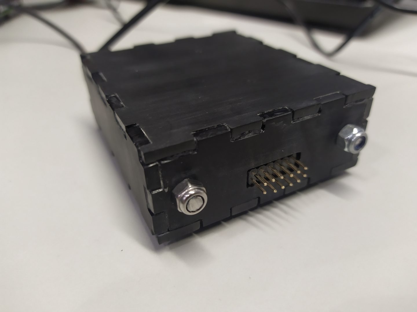
Figure 1: PMOD connector on the final design, height optimised for FPGA board.
As the objective here was to produce something for fairs and presentations, we also built a case for a handheld screen. Similar methods as in the the PMOD connector were used for the construction.
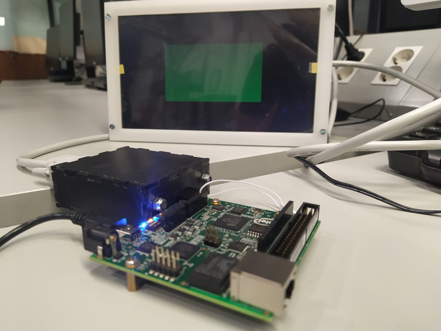
Figure 2: Complete final design, with PMOD to VGA connector and screen.
Hardware Design
We implemented a software based pseudo random number generator, RAM management module and a VGA interface on a development FPGA board. We used VHDL as the hardware description language for the design, the ModelSim software for running simulations with the testbenches implemented, and Intel’s Quartus Prime Lite software for synthesizing the design for uploading on the FPGA board.
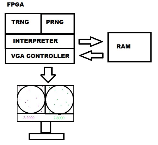
Figure 3: Overview of the project structure.
All different parts of the project work fine individually, but integration is not yet complete. Below is one of our sketches for visualizing random numbers on the screen.
![]()
Figure 4: Trying out different ways of drawing on the screen with our VHDL implementation.
FPGA boards are ideal for learning about the low level workings of electronics, and really understanding what goes into designing hardware. They are a useful tool also for learning about signals and communication between hardware – we especially enjoyed designing the VGA interface.
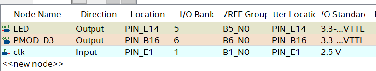
Figure 5: Mapping the VHDL elements in a blinking LED design to physical pins on the board in Quartus Prime Pin Planner.
Team

Matti Jämsen, student of Electrical Engineering at Aalto University
Special responsibilities: VGA connector and physical design

Virpi Sumu, student of Automation (switching to Electrical Engineering) at Aalto University
Special responsibilities: Project management, communication with company and reporting